Blogs and Insights
Blogs
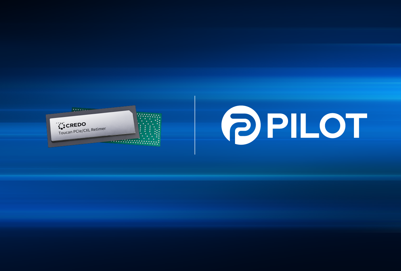
Building Stable PCIe Gen6 Systems
Blogs
Beyond Bandwidth: Why AI Infrastructure Needs an Observable Optical …
Blogs
Intelligent Connectivity: The Next Evolution of AI Infrastructure
Blogs
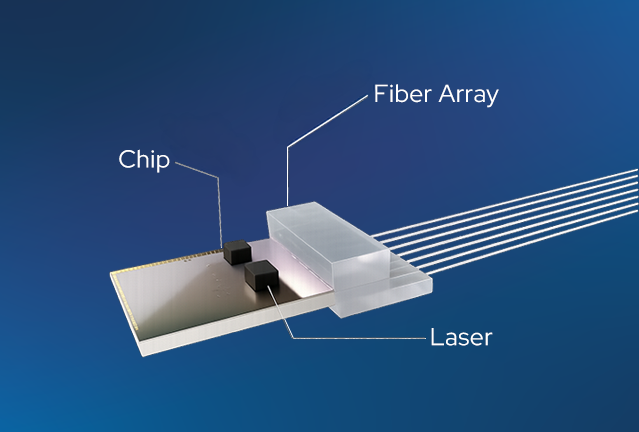
The Advantages of Low Loss Laser Coupling (L3C) …
Blogs
MicroLED Technology: Enabling New Reliable Interconnect Form Factors …
Blogs
Credo AECs Named “Data Center Solution of the …
Blogs
MicroLED Technology: Bringing Reliability, Longer Reach, and Lower Power to High-Throughput AI Fabrics
Blogs
OFC 2026 Highlights Critical Role of Reliability and …
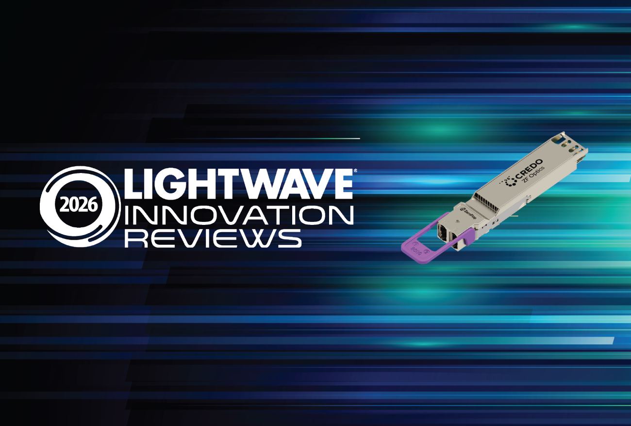
Blogs
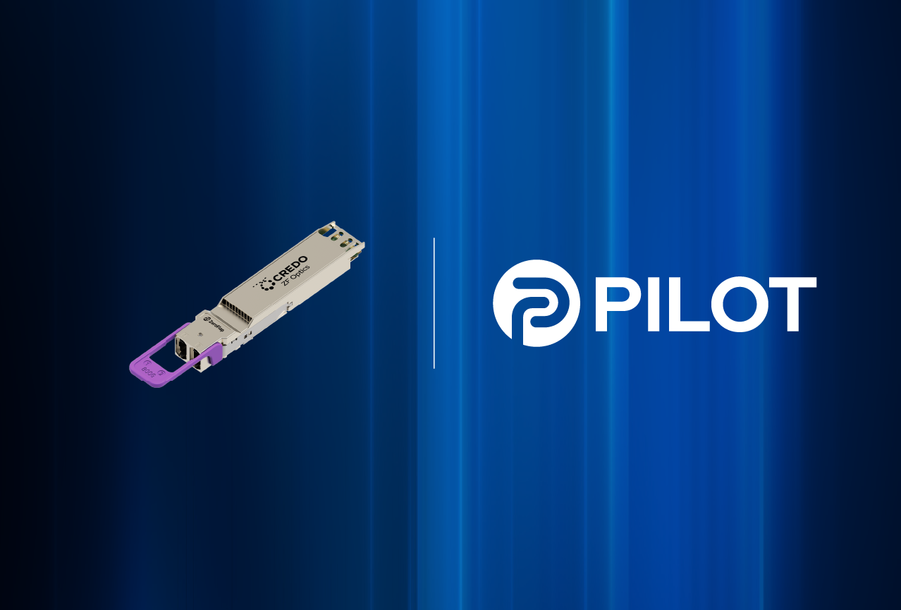
Credo’s ZeroFlap Optical Transceivers Receive 2026 Lightwave Innovation …


Reach out today to connect with Credo
Send us your inquiry and we will get back to you.
We have solutions