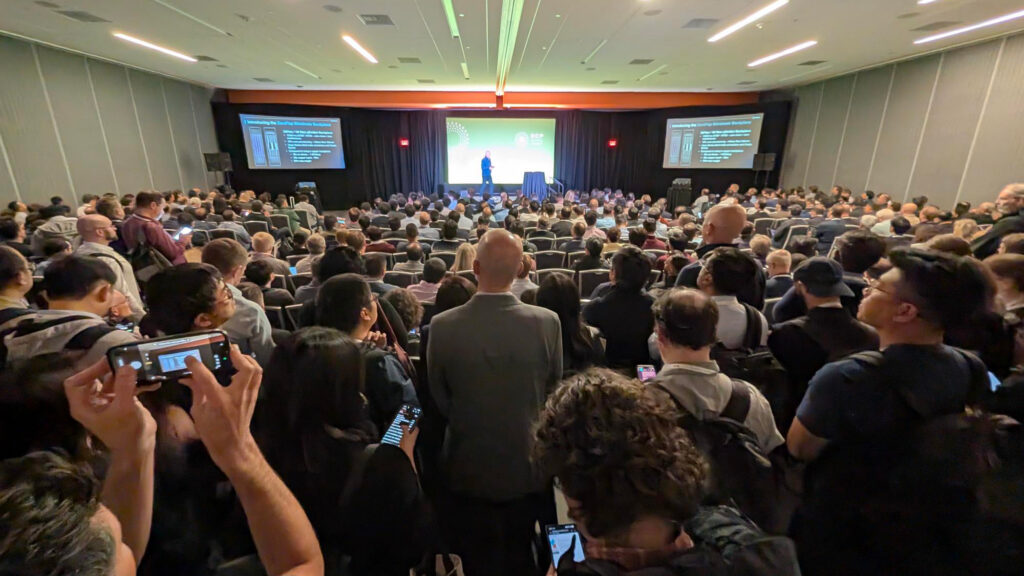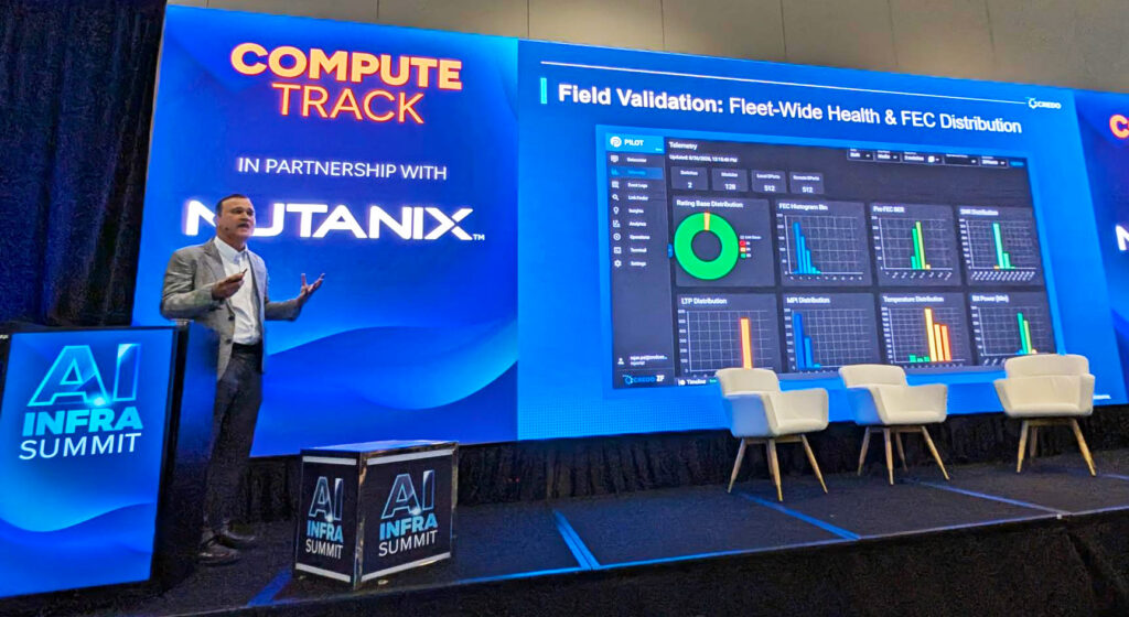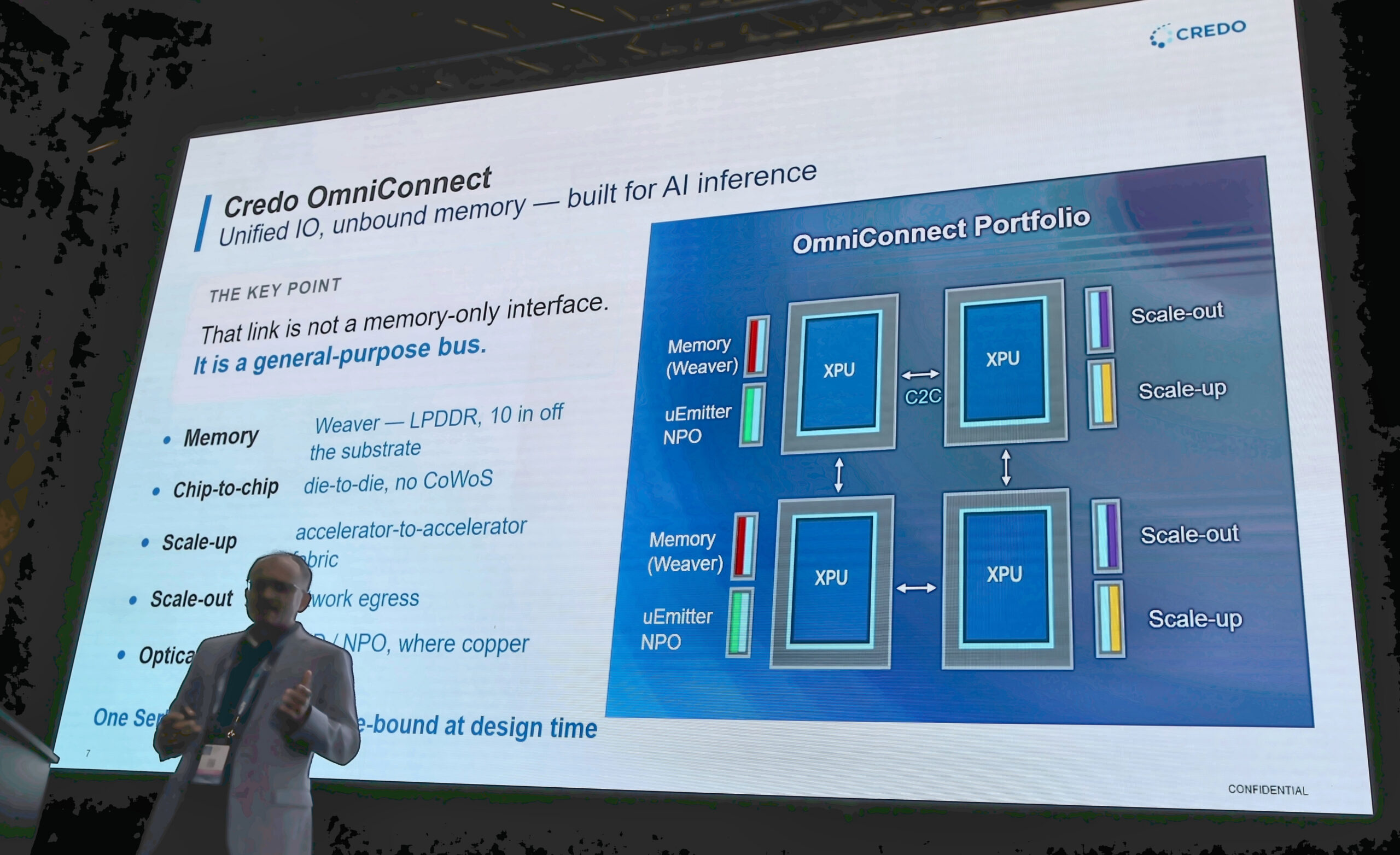
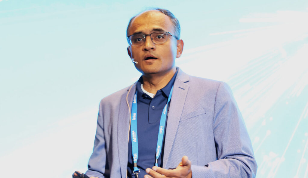
Credo VP of Product for OmniConnect and PCIe Vishal Shah introduces solutions to the memory wall at the 2026 AI Infra Summit.
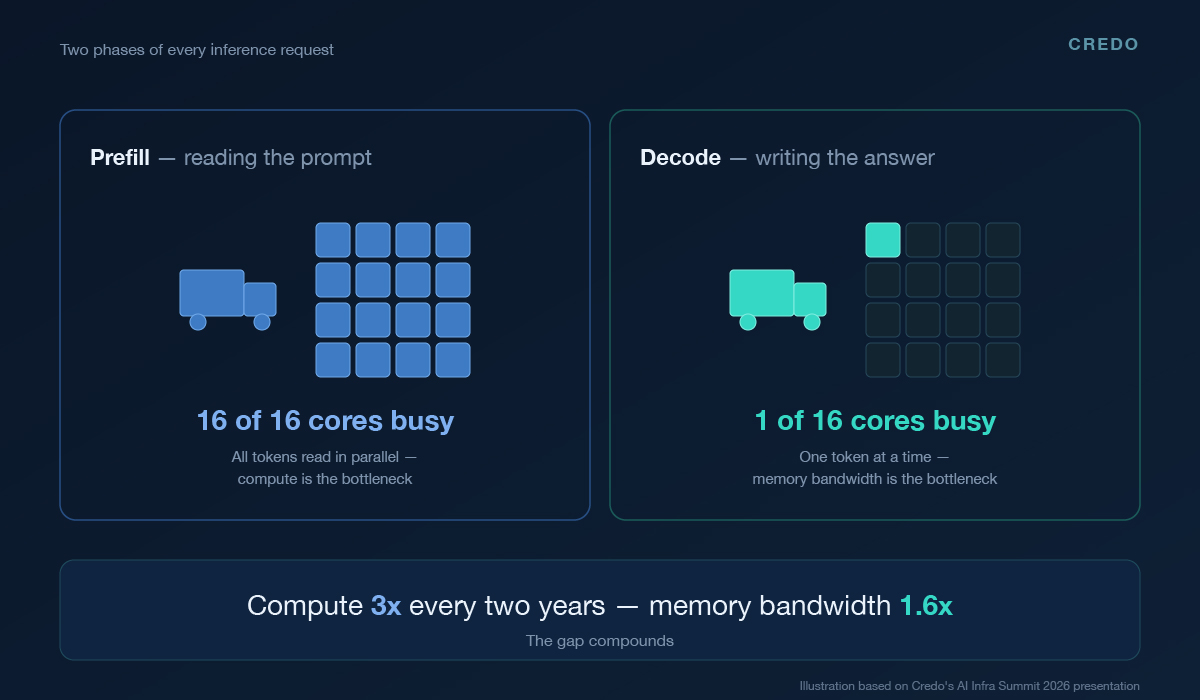
The Memory Wall is one of the more universal problems in AI infrastructure today — every team building or serving large models runs into some version of it, regardless of which accelerator they’ve standardized on. At AI Infra Summit 2026, Credo’s VP of Product for OmniConnect and PCIe, Vishal Shah, framed it with a metaphor: the factory hasn’t gotten smaller — compute keeps getting faster. What’s fallen behind is the delivery truck — memory’s ability to feed that compute fast enough to keep it busy.
“The thing that actually limits AI inference performance is memory. And the limit is physical.”
Two Stages, One Bottleneck
Inference runs in two phases with almost opposite characteristics.
Prefill reads the whole prompt at once. Every token is processed in parallel, and in a typical setup, all the compute cores stay busy. It’s a genuinely compute-bound stage.
Decode flips that around. Tokens come out one at a time, and producing each one means pulling the entire, growing key-value cache back out of DRAM. Only a fraction of those same cores stays busy while the rest sit idle waiting on data. It’s memory-bound, and because decode generates the majority of tokens in a real conversation or agent session, it’s the stage that shapes what a user actually experiences.
Compute has kept scaling fast: roughly 3x every two years. Memory bandwidth hasn’t kept pace, improving closer to 1.6x over the same period. That gap doesn’t reset each generation — it compounds.
Memory Demand Is Exploding
Three trends are pushing memory requirements up faster than that bandwidth gap alone would suggest, and they show up in every serving stack, not just one corner of the industry:
- Bigger Mixture of Experts (MoE) models. Total parameter counts can jump roughly 10x between generations even when the active parameters per token barely move. That’s a capacity problem since every expert still must be resident in memory whether or not it’s used on a given token.
- Long context and agents. The KV cache grows with every token, straining both capacity and bandwidth as agentic, multi-turn use cases push context length further out.
- Reasoning tokens. Chain-of-thought models can generate 10x to 100x more tokens per answer than a direct response — a bandwidth problem, since every one of those tokens runs through the memory-bound decode path.
Put together, the memory a serving instance needs to hold has climbed from roughly 0.4TB for 2020-class dense models, to about 1.2TB for 2023-era MoE models, toward something in the neighborhood of 5TB for 2026’s agentic workloads — around 12x growth in six years, for the same class of problem. The composition has shifted too: in 2020, the KV cache was a rounding error next to the model weights. By 2026, it rivals them.
The Physical Wall
The obvious answer — just put more memory on the package — runs into two limits that show up no matter which accelerator a system is designed around.
The first is substrate area. A typical 100mm × 100mm organic substrate, with LPDDR placed beside the compute die, tops out around 256GB. Swapping in HBM4 instead doesn’t solve it either — reticle limits mean an HBM4 alternative on that same substrate caps out well below what a serving instance now needs.
The second, more fundamental limit is what hardware engineers call beachfront: the usable perimeter of the compute die where memory interfaces can physically attach, measured in bandwidth per millimeter of die edge. LPDDR5X delivers about 0.18TB/s per millimeter; GDDR7 about 0.4. HBM4 is far denser, at roughly 2.0TB/s per millimeter — which is exactly why it’s become the default for peak bandwidth. But that density comes from advanced packaging, and packaging doesn’t change the fact that the perimeter itself is finite. Once it’s full, it’s full.
Both limits rest on the same assumption: memory must sit immediately next to the compute die. As Vishal framed it:
“Why not just add more memory? This is where physics gets in the way.”
Breaking Both Barriers
If proximity is the assumption creating the constraint, one way through is to relax it: serialize the connection, strip the protocol down to essentials, and let memory leave the package entirely.
That’s what Credo’s OmniConnect architecture does. On the substrate side, a Very Short Reach (VSR) SerDes link extends reach to roughly 250mm — about 10 inches — so memory is no longer limited to what fits beside the die. On the beachfront side, that same link packs in roughly 10x the die-edge density of parallel LPDDR, because a serial link needs far fewer pins to move the same data.
The remaining cost is latency, and it’s a real one: about 50 nanoseconds round trip, including forward error correction. To keep that number small, OmniConnect runs a stripped-down version of CXL — keeping the parts of the protocol that carry real value, like the FLIT structure, FEC, and credit-based flow control, while dropping the parts that exist for negotiation rather than throughput, like speed hopping and link renegotiation. The physical layer itself runs at around 0.75 picojoules per bit, low enough that the power budget doesn’t fight the latency budget. The result preserves the full semantics of local memory: whatever an XPU can do to memory sitting right next to it, it can do the same way over OmniConnect.
Matching HBM4’s Bandwidth, Not Its Ceiling
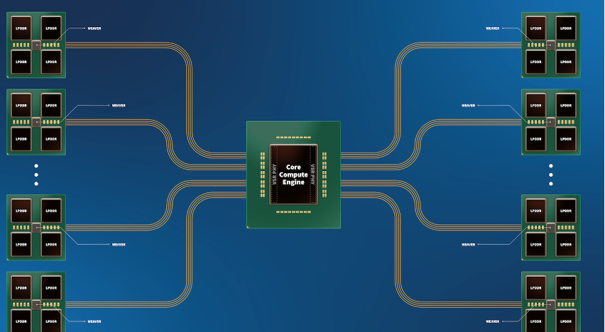
Weaver, the first product built on OmniConnect, is a memory fanout gearbox chiplet — it takes standard LPDDR and fans it out across that SerDes link instead of crowding it onto the substrate.
Die-edge to die-edge, Weaver matches HBM4’s bandwidth — 6.4TB/s against 6.1TB/s — while carrying roughly 25x the capacity: 4.8TB against HBM4’s 192GB, using dozens of small Weaver packages on a standard organic substrate instead of a handful of HBM stacks. No interposer, no CoWoS.
Just as important, Weaver doesn’t have to replace HBM — the two can share a package. An accelerator with two reticle dies and eight HBM4 stacks might use only 288GB and 22TB/s on-package, leaving roughly 10mm of edge unused. Weaver-connected LPDDR6 on that leftover edge adds another 1.5TB and 3.7TB/s, for a combined 1.8TB and 25.7TB/s — more of both, from the same package. Not a replacement for HBM; a way to use die edge that would otherwise go unclaimed.
Why Sustained Bandwidth Matters More Than Peak
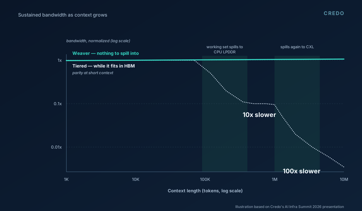
Peak bandwidth numbers assume the working set fits inside the fastest tier of memory. A conventional tiered hierarchy — SRAM, then HBM4, then CPU-attached LPDDR, then a CXL pool for the overflow — holds close to peak only while the KV cache fits inside HBM. Spill into LPDDR, and sustained bandwidth drops roughly 10x. Spill again into CXL, and it drops roughly 100x.
A single-hop architecture like Weaver skips that cliff — there’s nothing to spill into, since the working set already lives in one large, directly attached pool. Bandwidth stays flat from thousands of tokens to millions, which is exactly where tiered systems struggle most: long-context and agentic workloads.
Memory as a Part You Add, Not a Part You’re Stuck With
There’s a practical benefit here too. Today, DRAM typically ships welded to the compute die: the accelerator vendor buys, holds, and prices it, a single failed chip can scrap the far more expensive die next to it, and capacity is fixed the moment the part ships.
With Weaver, memory attaches over a standard VSR link and can be populated the way server DIMMs are — by the system integrator, at build time, rather than the chip vendor at tape-out. Either part can be replaced independently, and capacity can be chosen at build and upgraded later instead of locked in at chip design time. That means better serviceability, lower total cost of ownership, and forward compatibility as LPDDR generations turn over.
A Shared Problem Needs Solutions Built in the Open
Credo believes that the fix for the memory wall shouldn’t stay proprietary — it’s infrastructure the whole industry needs, the way high-speed Ethernet or PCIe became something everyone builds on rather than one company’s property. That’s why Credo contributed its lightweight AXI framing specification to the Open Compute Project in August 2026, forming the Lightweight Serial Interconnect Workstream inside OCP’s Open Chiplet Economy subproject — a standardized, open interconnect any accelerator vendor can build against, not a walled garden.
Where This Leaves Things
Vishal closed with three points worth repeating: inference is memory bound, with demand outrunning hardware by roughly 12x per serving instance in six years; the wall is physical but dissolves once you serialize the bus, gaining roughly 10 inches of reach and 10x the density per millimeter of die edge; and the result matches HBM’s bandwidth at roughly 25x the capacity, on standard packaging — additive to HBM, not a replacement for it.
Compute will keep getting faster. The open question is whether data can get to it fast enough to keep it fed. The memory wall is real and physical — but physical constraints get solved with better engineering, not by waiting them out. It’s a problem the industry now has a genuine, open path to solving together.